Nanochips a prueba de agua
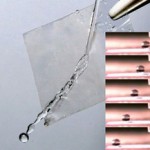
A single drop of water can be fatal to electrical circuits. To prevent water damage, current electronic devices are well sealed and packaged with polymer passivation. Researchers in Korea have now gone one step further and made water resistance a feature of the device itself by incorporating nonwetting, superhydrophobic components into the electronic device. They demonstrated this novel idea with a source/drain structure in a thin-film transistor.
Leer completo | Comentarios desactivados en Nanochips a prueba de agua
Celdas solares impresas en papel
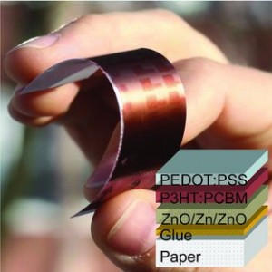
Polímero/fullereno para celdas solares impreso en masa en papel
Leer completo | Comentarios desactivados en Celdas solares impresas en papel
Angulo de contacto en nanopartículas
Investigadores del Laboratory of Surface Science and Technology en ETH Zurich desarrollan técnica para medir ángulo de contacto en nanopartículas tan pequeñas como 10nm.
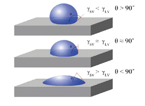 Contact angle is parameter essentially required for production of new material as it contains all vital information for predicting the behavior of the nanoparticles and now researchers at the Laboratory of Surface Science and Technology at ETH Zurich has successfully developed a procedure for measuring contact angle for nanoparticles as small as 10 nm.
The research finding has been recently published in the journal Nature Communications, where the researchers claim that they have studied liquid or fluid interfaces. Both hydrophilic and hydrophobic materials in the range of few nanometers were studies. The present method doesn’t allow measuring the contact angle below 500 nm and now researchers claim to have measured the contact angle even for very small and well below 500 nm nanoparticles.
Leer completo | Comentarios desactivados en Angulo de contacto en nanopartículas
Material autorreparable (con quitosana)
En el futuro quizás lo único que necesite para reparar la pintura de su auto será un rayo de sol.
Científicos en Estados Unidos crearon un nuevo material que, dicen, puede autoreparar sus roturas y rasguños cuando se le expone a un rayo de luz ultravioleta.
El secreto del material, afirman los investigadores en la revista Science, está en que utiliza moléculas hechas de chitosan, una sustancia natural que se deriva de las conchas y caparazones de crustáceos como el camarón.
Leer completo | Comentarios desactivados en Material autorreparable (con quitosana)
El transistor más pequeño… (en)
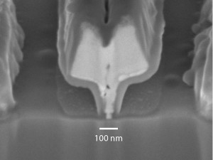
For the first time, researchers from CNRS France and ETH Zurich have succeeded in producing high-performance high-electron-mobility transistors (HEMTs) made of gallium nitride (GaN) on a silicon(110) wafer. (Photo: courtesy of C. Bolognesi / ETH Zürich)
El transistor de nitruro de galio más pequeño, rápido y económico
Researchers under ETH-Zurich professor Colombo Bolognesi are working on a new gallium nitride transistor technology using silicon(110) as a substrate. As the new combination of materials has many advantages, gallium nitride is poised to conquer the electronics market and help power the green revolution.
For the first time, researchers from CNRS France and ETH Zurich have succeeded in producing high-performance high-electron-mobility transistors (HEMTs) made of gallium nitride (GaN) on a silicon(110) wafer. This makes these transistors compatible with current complementary metal oxide semi-conductor (CMOS) chips based on silicon of the same crystal orientation. CMOS chips are generally produced on silicon wafers with the so-called (100) or (110) crystal orientation. GaN, on the other hand, could previously only be used on (111)-silicon until now. This new development makes it possible to construct hybrid electronic components that combine the computational power of the CMOS chip and the power handling capability of GaN transistors, which means power electronics can be made even more compact.
Leer completo | Comentarios desactivados en El transistor más pequeño… (en)
Material orgánico más fuerte… (en)
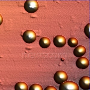
Equipo de nanotecnología reporta el material orgánico más fuerte jamás desarrollado. PRNewswire London September 29. TEL AVIV Israel
Equipo de nanotecnología reporta el material orgánico más fuerte nunca antes desarrollado
TEL AVIV, Israel, September 29, 2010 /PRNewswire/ — A revolutionary new spherical nanostructure, fully derived from very simple organic elements, yet strong as steel, has been developed and characterized at the laboratories of Ehud Gazit of Tel Aviv University and Itay Rousso of the Weizmann Institute of Science. Lightweight and exceptionally strong, easy and inexpensive to produce, friendly to the environment and biologically compatible, these promising bio-inspired nano-spheres have innumerable potential uses – from durable composite materials to medical implants. The groundbreaking work was recently published in the leading journal Angewandte Chemie.
Leer completo | Comentarios desactivados en Material orgánico más fuerte… (en)
